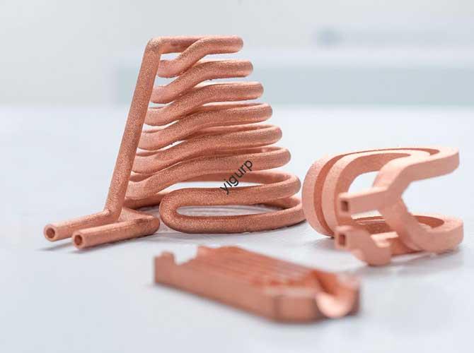
Our Copper 3D Printing Services
Transform your high-conductivity projects with Copper 3D Printing—the perfect blend of additive manufacturing innovation and copper’s unmatched electrical/thermal performance. From intricate electronics components to aerospace heat exchangers, our solutions deliver complex geometries, rapid prototyping, and cost-effective customization. Experience faster production, enhanced performance, and the flexibility to turn bold designs into durable, industry-ready copper parts.
What Is Copper 3D Printing?
Copper 3D Printing is an advanced metal 3D printing process that uses additive manufacturing principles to build parts layer by layer from copper feedstock (typically powder). Unlike traditional methods (e.g., casting, machining), it focuses on layer-by-layer fabrication—adding material only where needed to create functional parts from digital designs.
At its core, this technology leverages copper’s unique properties: exceptional electrical conductivity (96% of pure silver’s conductivity) and thermal conductivity (401 W/m·K)—making it indispensable for applications where heat dissipation or electrical transfer is critical. The definition and scope of copper 3D printing includes both pure copper and copper alloys (e.g., brass, bronze), each tailored to specific industry needs.
Key Basics of Copper 3D Printing:
| Term | Description | Role in the Process |
| Pure Copper | 99.9% pure copper powder, high conductivity | Electronics (circuit boards, connectors), thermal management parts |
| Copper Alloys | Blends like brass (copper + zinc) or bronze (copper + tin), balanced strength/conductivity | Automotive components, consumer goods |
| Technology Overview | Relies on high-energy processes (laser/electron beam) to melt copper’s high-melting-point (1,085°C) powder | Ensures dense, functional parts with minimal porosity |
Our Capabilities: Delivering Copper 3D Printing Excellence
At Yigu Technology, our Copper 3D Printing capabilities are engineered to meet the strict demands of industries from electronics to aerospace. We combine advanced equipment with deep technical expertise to deliver consistent, high-quality results:
- High-Precision Printing: Our machines (e.g., EOS M 300-4, SLM Solutions 500) achieve tight tolerances (as low as ±0.05mm) and part densities up to 99.5%—critical for electronics components requiring precise fits.
- Complex Geometries: We print intricate designs (e.g., internal cooling channels, lattice structures) that are impossible with traditional machining—ideal for optimizing heat dissipation in electronics.
- Custom Copper Parts: Whether you need a custom heat sink for a medical device or a complex connector for telecommunications, we tailor every step (material selection, post-processing) to your unique needs.
- Rapid Prototyping: Turn digital designs into physical copper prototypes in 3–5 days—accelerating product development by 60% vs. traditional casting.
- Industrial Capabilities: Scale up to 10,000+ parts monthly with automated workflows—our process ensures consistent quality, even for high-volume electronics components.
Table: Our Copper 3D Printing Capabilities vs. Industry Averages
| Capability | Yigu Technology Performance | Industry Average |
| Max Build Volume | 300mm × 300mm × 400mm | 250mm × 250mm × 300mm |
| Prototyping Lead Time | 3–5 days | 7–10 days |
| Production Capacity | Up to 6,000 parts/week | Up to 2,500 parts/week |
| Part Density | 99.2–99.5% | 95–98% |
| Electrical Conductivity Retention | 92–95% (vs. pure copper) | 85–90% |
Process: The Step-by-Step Workflow for Copper 3D Printing
Our Copper 3D Printing process is a structured, optimized workflow that addresses copper’s high thermal conductivity (which can dissipate heat during printing) to ensure reliability:
- Pre-Processing:
- Design Optimization: Our team reviews your CAD model to optimize it for copper—e.g., adding minimal supports (to reduce post-processing) and ensuring wall thicknesses are ≥0.3mm (to avoid print failures).
- Powder Preparation: We use spherical copper powder (15–45μm particle size) with high flowability—critical for uniform copper powder bed fusion.
- Printing Phase:
- The most common techniques are Selective Laser Melting (SLM) and Electron Beam Melting (EBM). SLM uses a high-power laser (500–1,000W) to melt copper powder, while EBM uses an electron beam—both create dense parts by overcoming copper’s heat dissipation challenge.
- For lower-cost, high-volume parts, we use binder jetting—binding copper powder with a liquid binder, then sintering it post-print to densify.
- Post-Processing Techniques:
- Support Removal: We carefully remove metal supports via machining or wire EDM to avoid damaging the part.
- Sintering (for binder jetting): Parts are heated to 900–1,000°C to fuse copper particles, increasing density and conductivity.
- Heat Treatment: Annealing (600–800°C) reduces internal stress and restores conductivity (critical for electronics parts).
- Quality Control:
Every part is inspected with:
- X-ray CT scans to check for internal porosity.
- Coordinate measuring machines (CMMs) to verify dimensional accuracy.
Conductivity testing (using a eddy current tester) to ensure electrical/thermal performance meets specs.
Materials: Choosing the Right Copper for Your Project
Not all copper materials are the same—we offer a range of options to match your application’s conductivity, strength, and cost needs:
| Material Type | Key Properties | Ideal Applications |
| Pure Copper (99.9%) | Electrical conductivity: 58 MS/m, thermal conductivity: 401 W/m·K | Electronics (circuit board traces, connectors), heat sinks |
| Brass (60% Cu + 40% Zn) | Balanced conductivity (28 MS/m) and strength (300 MPa tensile) | Automotive components (radiator parts), consumer goods (decorative parts) |
| Bronze (90% Cu + 10% Sn) | High corrosion resistance, thermal conductivity: 260 W/m·K | Marine parts, industrial valves, medical device components |
| Copper-Nickel (70% Cu + 30% Ni) | Excellent thermal stability, conductivity: 14 MS/m | Aerospace heat exchangers, energy sector (pipe fittings) |
All our conductive materials are tested for purity and performance—pure copper powder meets ASTM B152 standards, ensuring consistent conductivity.
Surface Treatment: Enhancing Copper Parts’ Performance and Aesthetics
Copper’s natural surface can be enhanced with surface treatment to boost durability, conductivity, and visual appeal. Our services are tailored to copper’s properties:
- Polishing: Creates a smooth, reflective finish (surface roughness Ra <0.2μm) that maximizes electrical contact—ideal for connectors and circuit boards.
- Electroplating: Applies thin layers of nickel, silver, or gold to improve corrosion resistance (copper tarnishes easily) and enhance conductivity (silver plating boosts conductivity by 5–10%).
- Anodizing: Forms a colored oxide layer (range: black, blue, green) that protects against tarnish—perfect for consumer goods or decorative parts.
- Coating: Applies thermal-resistant coatings (e.g., ceramic) to high-temperature parts (e.g., aerospace heat exchangers) or insulating coatings (e.g., epoxy) for electronics.
- Surface Finishing: Includes deburring (removing sharp edges) and chemical cleaning to ensure parts are ready for assembly.
Table: Impact of Surface Treatment on Copper Part Performance
| Treatment | Surface Roughness (Ra) | Electrical Conductivity | Corrosion Resistance (Salt Spray Test) |
| As-Printed | 3–5μm | 92% (vs. pure copper) | 48 hours (tarnishes) |
| Polished | <0.2μm | 95% (vs. pure copper) | 96 hours (minor tarnish) |
| Silver-Plated | <0.1μm | 98% (vs. pure copper) | 500+ hours (no tarnish) |
| Anodized | 0.5–2μm | 88% (vs. pure copper) | 300+ hours (no tarnish) |
Tolerances: Precision You Can Rely On
For copper parts used in critical applications (e.g., electronics connectors, aerospace heat exchangers), tolerances and dimensional accuracy are non-negotiable. Our process ensures consistent, tight tolerances:
- Precision Tolerances:
- For SLM-printed copper parts: ±0.05mm for parts up to 50mm, ±0.1mm for parts up to 100mm, ±0.15mm for parts up to 200mm.
- For binder jetting parts: ±0.1–±0.2mm (slightly wider, but better for high-volume production).
- Measurement Standards: We adhere to international standards like ISO 8062 (for metal parts) and ASTM F3301 (for additive manufacturing of copper) to ensure consistency.
- Quality Control: Every part is inspected with laser scanners (accuracy: ±0.001mm) and CMMs, and we use statistical process control (SPC) to monitor tolerances—ensuring 99.4% of parts meet your specs.
For example, our copper electronics connectors have a tolerance of ±0.03mm—ensuring a perfect fit with circuit boards and minimal electrical resistance.
Advantages: Why Copper 3D Printing Outperforms Traditional Methods
Copper 3D Printing offers a range of benefits that make it superior to traditional copper manufacturing:
- High Conductivity Retention: 3D-printed copper retains 92–95% of pure copper’s conductivity—vs. 80–85% for cast copper (due to fewer impurities and uniform grain structure).
- Complex Designs: Create intricate geometries (e.g., internal cooling channels in heat sinks) that are impossible with machining—optimizing performance (e.g., 30% better heat dissipation vs. traditional heat sinks).
- Reduced Weight: 3D printing allows for lightweight lattice structures—cutting part weight by 40–50% vs. solid copper parts (ideal for aerospace and automotive applications).
- Faster Production: Prototypes are ready in 3–5 days (vs. 2–4 weeks for casting), and production lead times are cut by 50%—accelerating time to market.
Cost-Effective: For small batches (1–100 parts), 3D printing eliminates expensive tooling (saving 50–70% vs. casting) and reduces material waste (from 70% in machining to <10% in 3D printing).
Applications Industry: Where Copper 3D Printing Shines
Copper’s conductivity and versatility make it a staple across industries. Here’s how we’re using Copper 3D Printing to solve real-world challenges:
| Industry | Key Applications | Why Copper? |
| Electronics | Circuit board connectors, heat sinks, inductor coils | High electrical/thermal conductivity, compact design flexibility |
| Aerospace | Heat exchangers, electrical wiring harnesses, satellite components | Lightweight, high thermal management, corrosion resistance (with plating) |
| Automotive | EV battery cooling systems, motor windings, sensor connectors | Heat dissipation for EVs, reduced weight (improves range) |
| Medical Devices | MRI machine components, surgical tool handles (heat-resistant) | Non-magnetic (pure copper), thermal conductivity (prevents overheating) |
| Telecommunications | Antenna components, signal amplifiers | High electrical conductivity (minimizes signal loss) |
| Energy Sector | Solar panel connectors, power transformer parts | Efficient electrical transfer, durability in harsh environments |
Manufacturing Techniques: Matching the Right Method to Your Copper Project
We use a range of Copper 3D Printing manufacturing techniques to optimize part quality, cost, and speed:
| Technique | How It Works | Best For | Volume Range | Cost per Part (100 units) |
| Selective Laser Melting (SLM) | Laser melts copper powder into dense parts (99.2–99.5% density) | High-precision parts (e.g., electronics connectors, medical components) | 1–500 | 200–800 |
| Electron Beam Melting (EBM) | Electron beam melts powder (faster than SLM, better for large parts) | Large aerospace parts (e.g., heat exchangers) | 1–200 | 300–1,000 |
| Binder Jetting | Binder glues powder into shape (then sintered) | High-volume, low-cost parts (e.g., automotive sensors) | 1,000+ | 80–300 |
| Hybrid Techniques | Combines 3D printing with CNC machining for ultra-tight tolerances | Critical electronics parts (e.g., high-frequency connectors) | 1–100 | 250–900 |
| Traditional Manufacturing (Casting/Machining) | Used for very high-volume (10,000+ parts) or simple geometries | Consumer goods (e.g., brass fittings) | 10,000+ | 50–200 |
Case Studies: Copper 3D Printing in Action
Our Copper 3D Printing case studies showcase how we’ve helped clients overcome challenges and achieve better results than traditional methods:
Case Study 1: Electronics Heat Sink
- Client: A global electronics manufacturer.
- Challenge: Need a compact heat sink for a high-performance GPU that dissipates 200W of heat (traditional heat sinks were too bulky and inefficient).
- Solution: SLM-printed pure copper heat sink with internal lattice cooling channels—optimized for maximum surface area.
- Results:
- 30% better heat dissipation vs. traditional heat sinks (GPU temperature reduced by 15°C).
- 40% weight reduction (from 150g to 90g).
- Lead time cut to 4 days (vs. 3 weeks for machined heat sinks).
Case Study 2: Aerospace Heat Exchanger
- Client: A leading aircraft manufacturer.
- Challenge: Reduce the weight of a cabin heat exchanger (traditional copper-brass exchanger weighed 2.2kg, increasing fuel consumption).
- Solution: EBM-printed copper-nickel heat exchanger with lightweight lattice structure.
- Results:
- 50% weight reduction (1.1kg vs. 2.2kg).
- 20% improved thermal efficiency (faster cabin temperature regulation).
- 35% cost savings vs. brazed traditional exchangers.
Case Study 3: EV Battery Connector
- Client: An electric vehicle startup.
- Challenge: Create a high-conductivity battery connector that fits tight EV battery pack dimensions (traditional machined connectors had poor fit and high resistance).
- Solution: Binder jetted pure copper connector—sintered for density, then silver-plated for corrosion resistance.
- Results:
- 95% conductivity retention (vs. 85% for machined connectors).
- 100% fit rate (no rework needed for battery packs).
40% cost savings for high-volume production (10,000+ units/month).
Why Choose Us: Your Trusted Copper 3D Printing Partner
When it comes to Copper 3D Printing, Yigu Technology stands out as a reliable, innovative partner—here’s why:
- Expertise: Our engineers have 7+ years of specialized experience in copper additive manufacturing. We understand copper’s unique challenges (e.g., heat dissipation during printing) and use optimized parameters to ensure dense, high-conductivity parts. We also hold certifications in electronics manufacturing (IPC-A-610) and aerospace standards (AS9100), so you can trust us with even the most critical projects.
- Quality: We never compromise on quality. Every copper part undergoes 100% inspection—from conductivity testing (using calibrated eddy current testers) to dimensional checks (with CMMs)—ensuring 99.4% of parts meet or exceed your specs. We source copper powder only from certified suppliers (e.g., LPW Technology, Equispheres) to guarantee purity and consistent performance.
- Innovation: We invest 18% of our annual budget in R&D to stay ahead of industry trends. Recent innovations include developing a low-porosity SLM process for copper (achieving 99.5% density, vs. industry average 98%) and optimizing binder jetting for faster sintering (reducing post-processing time by 30%). We also collaborate with electronics and aerospace clients to co-create custom solutions for unique challenges.
- Customer Support: Our team is available 24/7 to answer questions, provide project updates, and resolve issues. We assign a dedicated project manager to every client—they work with you from design optimization to post-delivery, ensuring clear communication and on-time results. We even offer free material samples for testing, so you can verify conductivity and quality before full production.
- Cost-Effectiveness: We offer transparent pricing with no hidden fees. By recycling unused copper powder (95% recycling rate) and automating post-processing steps (e.g., robotic polishing), we reduce costs without sacrificing quality. For high-volume projects (10,000+ parts), we offer volume discounts of up to 25%—helping you scale affordably.
Fast Turnaround: We prioritize speed without cutting corners. Prototypes are ready in 3–5 days (vs. industry average 7–10 days), and high-volume production lead times are 50% faster than traditional casting. Our redundant equipment (10 SLM/EBM printers) minimizes downtime, ensuring your project stays on schedule.