In today’s fast-moving electronics market, speed wins. Moving from a digital concept to a tangible, test-ready model is a major hurdle. Old-school methods are slow, costly, and rigid. This is where 3D printed electronic digital prototype models change the game. They use additive manufacturing to build parts layer-by-layer straight from a CAD file. This guide breaks down how it works, its key benefits, and real uses. You will see how it cuts time, slashes cost, and boosts design freedom for engineers and startups.
How Does the 3D Printing Process Work for Electronic Prototypes?
It’s more than just printing plastic. It’s a direct path from your computer screen to a part you can hold and test. Here is a simple step-by-step look.
Step 1: What Digital File Do You Need?
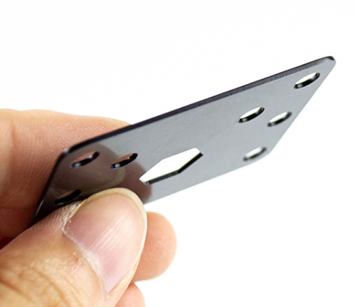
You start with a final 3D CAD model. Tools like SolidWorks or Fusion 360 are used to design the product. Think of a smartphone case, sensor box, or a drone arm. The file must be very precise. It needs details for ports, screws, and space inside for circuits and batteries.
Step 2: Why Does Material Choice Matter So Much?
Picking the right material is key for a useful prototype. Your choice depends on what you need to test. Below is a quick guide.
| Material Type | Best For These Prototypes | Key Property |
|---|---|---|
| ABS Plastic | Laptop chassis, tool handles | Strong, impact-resistant |
| UV-Cured Resin | Small sensor cases, fine details | Smooth surface, high detail |
| Metal Alloys | Heat sinks, motor housings | Handles high heat, very strong |
Step 3: How Is the Part Actually Printed?
Special software cuts the CAD model into thin layers. A 3D printer then builds the part one layer at a time. It uses heat or light to melt or cure the material. A full prototype can be ready in hours, not weeks. No molds or special tools are needed.
Step 4: What Happens After Printing (Post-Processing)?
The part comes off the printer and gets cleaned. Support material is removed. It might be sanded or painted. Then, real electronic parts like PCBs, wires, and batteries are added for testing. This step makes the model truly functional.
A Real Case: A tech firm needed a new router case prototype. The old way (injection molding) took 5 weeks and $7,000 for the mold alone. With 3D printing, they had a working model in 2 days for under $200.
Why Are 3D Printed Prototypes a Game-Changer for R&D Teams?
For product teams, the main goals are speed, low cost, and the freedom to change designs. 3D printing hits all three. Let’s look at the direct comparison.
| Key Benefit | Traditional Method (e.g., Injection Molding) | 3D Printed Prototyping | Impact for Your Team |
|---|---|---|---|
| Time to First Prototype | 4 to 8 weeks | 1 to 3 days | Cut R&D cycles by over 90% |
| Upfront Cost | $5,000 – $20,000+ (for tooling) | $50 – $500 (per part) | Save 95% on initial costs |
| Design Changes | Hard and costly (new mold needed) | Easy and fast (edit CAD file) | Test 5-10 ideas instead of just 1 or 2 |
A Real-World Example: A team was making a smart wearable device. The first design was bulky and blocked Bluetooth signals. With old methods, a new mold would cost $8,000 and take 6 weeks. Using 3D printing, they changed the CAD file in an afternoon. They printed three new versions in 48 hours for about $100 each. They tested them, made one more tweak, and had a perfect model in under 10 days. This saved them thousands of dollars and over a month of time.
What Are the Key Uses for These Prototypes?
This tech is useful at every stage of making a new electronic product.
Use 1: How Can You Validate Your Concept Early?
Before big money is spent, you need to check the look and feel. 3D prints let you:
- Hold a model of a new game controller to check grip comfort.
- See if all the internal parts fit inside a tablet’s housing.
- Show a realistic model to investors or bosses for quick approval.
Use 2: How Do You Test for Function and Durability?
Once the design is set, you need to test how it works in the real world.
- Drop Testing: Use a strong plastic (like ABS) to make a phone case and test its strength.
- Heat Testing: Print a heat sink from metal to see if it keeps a computer chip cool.
- Signal Testing: Check if a resin antenna cover blocks Wi-Fi or cellular signals.
Use 3: Can You Use It for Small Production Runs?
Yes. For custom or limited items, 3D printing is perfect for small batches.
- A medical device company prints 10-20 custom hearing aid shells for each patient.
- A startup makes 500 limited-edition smart speakers for a pre-launch market test.
Conclusion
3D printed electronic prototype models are not just a handy tool. They are a core strategy for modern product development. They solve the big problems of slow speed, high cost, and rigid design. By letting you iterate fast and test cheaply, they reduce risk and help get better products to market sooner. As materials improve, this link between prototype and final product will only grow stronger.
FAQ
1. Can 3D printed prototypes handle real functional tests?
Yes. Today’s materials are strong. You can use them for drop tests, heat tests, and signal tests. You can also install real circuit boards and batteries into the printed parts for full function testing.
2. Is 3D printing good for making lots of prototypes?
It is best for small to medium runs (1 to 100 units). For making 500 or more of the same part, methods like injection molding may become cheaper. But for testing many design changes or making custom parts, 3D printing is still the best choice.
3. What is a common mistake when 3D printing prototypes?
People skip post-processing. Printed parts often need cleaning, sanding, or curing. If you don’t do this, parts might not fit together right. This can ruin your test results, like a button that doesn’t click because the hole is too rough.
Discuss Your Electronic Projects with Yigu Rapid Prototyping
Do you have a new electronic product in mind? Are you stuck by slow prototypes or high costs? Let’s talk. At Yigu, we use advanced 3D printing to help teams like yours move faster. We can help you test designs, check function, and refine your product with speed and precision. Share your project goals with us, and see how rapid prototyping can give you the edge.