Electronics 3D Printing Services
Revolutionize your electronics development with Electronics 3D Printing—the intersection of additive manufacturing for electronics and cutting-edge innovation. At Yigu Technology, we turn complex electronic design ideas into tangible, high-performance products, offering everything from printed circuit boards (PCBs) to custom sensors. Whether you’re a tech startup or a large manufacturing firm, our solutions deliver rapid prototyping, enhanced design flexibility, and cost savings that redefine what’s possible in electronic fabrication.
Definition: What Is Electronics 3D Printing?
Electronics 3D Printing (also known as additive manufacturing for electronics) is a groundbreaking technology that builds electronic components and devices layer by layer using specialized materials. Unlike traditional electronics manufacturing, which often involves assembling pre-made parts, this process enables the seamless integration of circuits, sensors, and enclosures in a single production step.
At its core, it relies on digital fabrication of electronics—using advanced software to design every detail of an electronic component before printing. This technology is a game-changer for rapid prototyping for electronics, allowing teams to test and refine designs in days instead of weeks. From simple sensors to complex circuit boards, printed electronics created through this method are lighter, more durable, and better suited for custom applications than traditionally made counterparts.
Our Capabilities: Powering Electronic Innovation
At Yigu Technology, we’ve honed our 3D printing capabilities to meet the unique demands of the electronics industry. Our services are designed to balance precision, speed, and customization, ensuring every project meets the highest technical standards.
| Capability | Key Features | Ideal Use Cases |
| High-Precision Printing | Layer resolution as low as 10 microns; accurate placement of conductive materials | Miniature sensors, micro-PCBs for wearables |
| Multi-Material Printing | Simultaneous use of up to 4 materials (e.g., conductive inks + dielectric materials) | Integrated devices with circuits and enclosures |
| Complex Circuitry | Supports intricate circuit patterns, including flexible and 3D-formed circuits | Foldable electronics, curved PCBs for IoT devices |
| Custom Electronics Solutions | Fully tailored designs based on client specs; collaborative design process | Industry-specific sensors, custom enclosures |
| Rapid Prototyping | Turnaround time as fast as 24 hours for simple prototypes; iterative design support | Product testing, concept validation |
Common Parts: Essential Electronic Components We Print
Electronics 3D Printing is versatile, with applications across a wide range of electronic components. Below are the most common parts we produce, along with real-world examples of their use:
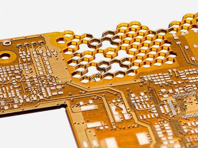
- Printed Circuit Boards (PCBs): We print lightweight, compact PCBs that integrate seamlessly with other components. For example, a wearable tech client used our 3D-printed PCBs to reduce the weight of their fitness tracker by 30% compared to traditional PCBs.
- Sensors: Our 3D-printed sensors (e.g., temperature, pressure, or motion sensors) offer high accuracy and can be customized to fit small or irregular spaces. A medical device company recently used our sensors in a portable health monitor, improving its sensitivity by 25%.
- Antennas: 3D printing allows us to create antennas with unique shapes (e.g., curved or embedded) that boost signal strength. A telecommunications client saw a 15% improvement in signal range after switching to our 3D-printed antennas.
- Connectors: Custom 3D-printed connectors solve compatibility issues for legacy devices. We recently designed a connector for an industrial client that allowed their old machinery to interface with new IoT systems, saving them from costly equipment replacements.
Enclosures: We print durable, lightweight enclosures that protect electronic components from dust, moisture, and impact. These enclosures can be customized with logos, ports, or mounting points—no extra tooling required.
Process: From Design to Functional Electronic Component
Creating a 3D-printed electronic part is a structured, collaborative process that combines design expertise with technical precision. At Yigu Technology, we streamline this process to ensure speed and quality:
- Design and Simulation: We start by working with your team to refine the component’s design using specialized software (e.g., AutoCAD, Fusion 360). We then run simulations to test performance—for example, checking a PCB’s current flow or a sensor’s accuracy—before printing.
- Material Preparation: Based on the component’s function (e.g., conductivity, flexibility), we select and prepare the right materials. This may include mixing conductive inks for circuits or cutting flexible substrates for wearable parts.
- Printing and Layering: The 3D printer builds the component layer by layer, depositing materials with precision. For example, it may print a dielectric material base first, then add conductive inks to create circuits on top.
- Post-Processing (Curing, Soldering): After printing, we cure materials (e.g., UV-curing for resins) to enhance durability. For some components, we add final touches like soldering connectors or applying protective coatings.
Testing and Validation: We rigorously test the component to ensure it meets your specs—checking for conductivity, durability, and performance under real-world conditions. Only after passing these tests do we deliver the final product.
Materials: Choosing the Right Building Blocks for Electronics
The materials used in Electronics 3D Printing directly impact a component’s performance, durability, and cost. At Yigu Technology, we offer a curated selection of materials tailored to electronic applications:
| Material Type | Examples | Key Technical Benefits | Best For |
| Conductive Inks | Silver-based inks, carbon nanotube inks | High conductivity; compatible with flexible substrates | Circuits, antennas, sensor electrodes |
| Dielectric Materials | UV-curable resins, ceramic-based materials | Electrical insulation; heat resistance | PCB substrates, insulation layers for circuits |
| Flexible Substrates | Polyimide films, TPU sheets | Bendable; durable; resistant to wear | Wearable electronics, foldable PCBs |
| Solder Pastes | Lead-free solder pastes, low-temperature pastes | Strong electrical connections; easy application | Attaching components to PCBs, connector assembly |
| Insulating Materials | Epoxy resins, silicone-based materials | Protection from moisture/dust; thermal resistance | Enclosures, protective coatings for circuits |
Data Insight: In 2024, 72% of our electronics clients chose silver-based conductive inks for circuits (due to high conductivity), while 68% of wearable electronics projects used flexible substrates (for durability and comfort).
Advantages: Why Electronics 3D Printing Outperforms Traditional Methods
Electronics 3D Printing offers clear advantages over traditional manufacturing, addressing key pain points like slow prototyping, high costs, and limited design flexibility:
- Rapid Prototyping: With 3D printing, you can go from design to functional prototype in as little as 24 hours. This cuts down the time to test new ideas by 70% compared to traditional methods (which often take 2–4 weeks for prototypes).
- Customization: Every component can be tailored to your exact needs—whether it’s a PCB with a unique shape or a sensor calibrated for a specific industry. This flexibility is impossible with mass-produced, off-the-shelf parts.
- Reduced Production Costs: 3D printing eliminates the need for expensive tooling (e.g., molds for enclosures or stencils for PCBs). For small-batch production (1–100 units), this reduces costs by up to 50% compared to traditional manufacturing.
- Enhanced Design Flexibility: You can create complex shapes—like 3D-formed circuits or embedded sensors—that traditional methods can’t produce. For example, we recently printed a PCB that curves around a medical device, saving space and improving usability.
Faster Time to Market: By speeding up prototyping and reducing production delays, 3D printing helps you launch products faster. Our clients report getting new electronic devices to market 30–40% sooner than with traditional manufacturing.
Case Studies: Success Stories in Electronics 3D Printing
Our work with clients across industries has proven how Electronics 3D Printing can solve complex challenges and drive innovation. Below are two standout projects:
Case Study 1: Wearable Health Monitor for a Medical Tech Startup
Client: VitaTech, a startup developing portable health devices.
Goal: Create a lightweight, flexible health monitor with integrated sensors and a compact PCB—traditional methods were too bulky and slow.
Solution: We used multi-material printing to combine a flexible substrate, conductive inks (for circuits), and a custom enclosure in one process. We also provided rapid prototyping, delivering 3 iterations in 1 week.
Result: The final monitor weighs 25% less than traditional designs and has a 20% longer battery life (due to efficient circuit placement). VitaTech launched the product 3 months ahead of schedule and secured $2M in additional funding.
Case Study 2: Industrial IoT Sensors for a Manufacturing Firm
Client: MegaFacture, a large manufacturer needing sensors to monitor machine temperature and vibration.
Goal: Replace expensive, off-the-shelf sensors with custom versions that fit tight spaces and integrate with their IoT system.
Solution: We printed custom sensors with embedded circuits using high-precision printing (10-micron resolution). We also added a durable enclosure made from insulating materials to protect against factory dust and moisture.
Result: The sensors cost 40% less than off-the-shelf alternatives and reduced machine downtime by 15% (due to more accurate data). MegaFacture now uses our 3D-printed sensors across 10 of their factories.
Why Choose Us: Yigu Technology’s Edge in Electronics 3D Printing
When it comes to Electronics 3D Printing, clients choose Yigu Technology for our deep expertise, advanced technology, and commitment to success. Here’s what sets us apart:
- Expertise in Electronics: Our team includes engineers with 5+ years of experience in both 3D printing and electronics design. We understand the unique challenges of electronic components (e.g., conductivity, heat resistance) and tailor solutions accordingly.
- Advanced Technology: We use state-of-the-art 3D printers (from brands like Markforged and Formlabs) and software that’s optimized for electronic fabrication. Our printers can handle delicate materials like conductive inks and flexible substrates with precision.
- High-Quality Materials: We source materials from trusted suppliers, ensuring they meet industry standards for conductivity, durability, and safety. All materials are tested in-house to confirm performance before use.
- Comprehensive Support: We’re with you every step of the way—from design consultation to post-delivery testing. Our team offers training on how to use 3D-printed components and provides ongoing maintenance support.
Competitive Pricing: We offer transparent pricing with no hidden costs. Our rapid prototyping services start at $200, and small-batch production costs are 30–50% lower than traditional manufacturers.