En el vertiginoso mundo del desarrollo de productos electrónicos digitales, pasar de un concepto de diseño a algo tangible, El prototipo comprobable es decisivo.. Los retrasos en la creación de prototipos pueden significar la pérdida de ventanas de mercado, mientras que los métodos de producción inflexibles pueden sofocar la innovación. Ahí es donde3D printed electronic digital prototype models come in. Esta tecnología se ha convertido en una piedra angular para los ingenieros., diseñadores, y empresas, solving key pain points in R&D by combining speed, precisión, y rentabilidad. Abajo, we’ll break down how it works, its core benefits, aplicaciones del mundo real, and why it’s essential for modern electronic product development.
How 3D Printing Creates Electronic Digital Prototype Models: A Step-by-Step Breakdown
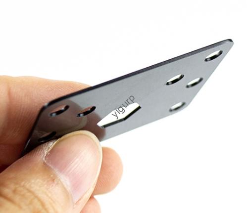
3D printing for electronic digital prototypes isn’t just about “printing a plastic part”—it’s a streamlined process that turns digital designs into functional, test-ready models. A diferencia de la fabricación tradicional (which requires expensive molds or complex tooling), 3D printing uses anfabricación aditiva approach: building parts layer by layer from digital files. Here’s a simple, desglose procesable del proceso:
- Digital Design Finalization: Engineers start with a 3D CAD (Diseño asistido por computadora) file of the electronic product (p.ej., a smartphone casing, a wearable sensor, or a circuit board housing). Tools like SolidWorks or Fusion 360 are used to refine details—such as port placements, internal cavities for components, or structural supports.
- Selección de materiales: For electronic prototypes, the right material is critical. Las opciones comunes incluyen:
- Plástico ABS: Ideal for durable, impact-resistant parts (p.ej., laptop chassis prototypes).
- Resinas (UV-Curable): Perfect for high-detail parts (p.ej., small sensor enclosures with fine grooves).
- Aleaciones metálicas (p.ej., Aluminio, Titanio): Used for heat-resistant or high-strength prototypes (p.ej., drone motor housings).
- 3D Printer Setup: The CAD file is sliced into thin layers (usually 0.1–0.3mm thick) using software like Cura. The printer then heats or cures the material layer by layer, following the sliced design.
- Postprocesamiento: Después de imprimir, the prototype is cleaned (p.ej., removing excess resin or support structures) and may be sanded or painted to mimic the final product’s appearance. For functional testing, componentes electronicos (like PCBs or batteries) are often integrated at this stage.
This process eliminates the need for tooling, which can take weeks or months with traditional methods. Por ejemplo, a simple smartphone casing prototype that once took 4–6 weeks to make with injection molding can now be 3D printed in24–48 horas.
Why 3D Printed Electronic Digital Prototypes Are a Game-Changer for R&D
For electronic product teams, the goal of prototyping is clear: validate designs, funcionalidad de prueba, and gather feedback fast.3D printed prototypes excel at this by addressing three core R&D challenges: tiempo, costo, y flexibilidad. Let’s quantify these benefits with data and examples:
| Beneficio | Traditional Prototyping (p.ej., Moldeo por inyección) | 3D Printed Prototyping | Key Impact for Electronic Products |
|---|---|---|---|
| Time to Prototype | 4–8 semanas (due to mold creation) | 1–3 días (direct from CAD file) | Cut R&D timelines by 90%—launch products faster. |
| Cost for Small Runs | $5,000–$20,000 (mold tooling alone) | $50–$500 per prototype (material + mano de obra) | Reduce upfront costs by 95%—test more designs. |
| Flexibilidad de diseño | Limited (molds can’t easily be modified) | Alto (CAD files edited in hours; no tooling changes) | Test 5–10 design iterations vs. 1–2 traditionally. |
Ejemplo del mundo real: Wearable Tech Startup
A startup developing a smart fitness tracker faced a problem: their initial prototype’s wristband was uncomfortable, and the sensor housing blocked signal. With traditional prototyping, fixing this would have required a new mold ($8,000) y 6 weeks of waiting. Instead, they used 3D printing:
- They edited the CAD file to adjust the wristband’s curvature and sensor housing shape (2 hours of work).
- Printed 3 new prototypes in 3 días ($120 total).
- Tested with users, refined once more, and had a final prototype ready in 1 semana.
This saved them $7,880 y 5 weeks—critical for a small team racing to launch.
Key Applications of 3D Printed Electronic Digital Prototypes
3D printing isn’t just for “quick fixes”—it’s used across the entire electronic product lifecycle, from early concept testing to pre-production. Here are the most common, high-impact use cases:
1. Concept Validation (Early-Stage R&D)
Before investing in full-scale production, teams need to confirm that a design “works” visually and ergonomically.3D printed prototypes let them:
- Test how a product feels in hand (p.ej., a wireless earbud’s weight and shape).
- Check if components fit (p.ej., a battery pack inside a tablet prototype).
- Gather stakeholder feedback fast (p.ej., showing a 3D printed smartwatch case to executives for approval).
2. Pruebas funcionales (Mid-Stage R&D)
Una vez finalizado el diseño, prototypes are used to test performance under real conditions. For electronic products, this includes:
- Durability Testing: Dropping a 3D printed smartphone prototype to check for structural damage.
- Thermal Testing: Using heat-resistant 3D printed parts (p.ej., metal alloy CPU coolers) to test how a laptop handles overheating.
- Signal Testing: Ensuring 3D printed antenna housings don’t block Wi-Fi or Bluetooth signals.
3. Small-Batch Production (Pre-Launch)
For products that need rapid iteration or personalized designs (p.ej., custom medical devices or limited-edition gadgets), 3D printing enableslow-cost small-batch production:
- A company making custom hearing aids uses 3D printing to produce 10–20 prototypes per patient, tailoring the fit to their ear canal.
- A tech brand creating a limited-edition gaming mouse printed 500 prototypes to test different grip styles before mass production.
Yigu Technology’s Perspective on 3D Printed Electronic Digital Prototypes
En Yigu Tecnología, we’ve seen firsthand how 3D printed electronic digital prototype models transform our clients’ R&D workflows—especially for startups and mid-sized enterprises. Many of our partners once struggled with long lead times and high tooling costs, which slowed their ability to innovate. Con impresión 3D, they now test 3–4 design iterations in the time it took to make one traditional prototype. We believe this technology isn’t just a “nice-to-have”—it’s a necessity for staying competitive in electronics. As 3D printing materials (like conductive resins for circuit boards) advance, we’ll see even more integration between prototyping and final production, making the gap from design to market even smaller.
Preguntas frecuentes:
1. Can 3D printed electronic prototypes handle real-world functional testing?
Sí! While early 3D prints were often “visual only,” modern materials (like high-temperature resins or metal alloys) are durable enough for rigorous testing—including drop tests, thermal cycling, and even basic electrical integration (p.ej., mounting PCBs in 3D printed housings).
2. Is 3D printing cost-effective for large-scale electronic prototype runs?
3D printing shines for small to medium runs (1–100 prototypes). para tiradas de 500+ unidades, traditional methods like injection molding may become cheaper—but 3D printing is still better for rapid iteration or personalized designs (p.ej., custom-sized medical devices).
3. What’s the most common mistake teams make when 3D printing electronic prototypes?
Skipping post-processing! Even high-quality 3D prints need cleaning (p.ej., removing resin residue) or minor sanding to ensure components fit properly. Forgetting this step can lead to inaccurate test results (p.ej., a sensor not aligning with a 3D printed housing).